
EUV Lithography
Overview
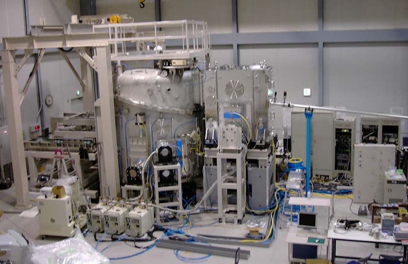
Research system for the development of "EUV absolute Wave Front metrology"
supported by NEDO Key Technology Research Promotion
EUV (Extreme Ultraviolet) Lithography is the leading technology candidate for manufacturing semiconductor devices in the next 50 nm generation. Using EUV of around 13.5 nm wavelength, projection of optical system with numerical aperture of 0.25 realizes high resolution of 30 nm or less. The purpose of this research is to develop a wave front measurement technology of optical components of the EUV exposure system, which is essential for the fabrication of future EUVL systems.
To realize EUVL for making semiconductor circuits with minimum line width of 50 nm or less, it is necessary to manufacture multilayer mirrors for reflection optics and multilayer masks for projection optics with surface roughness and shape accuracy around 0.1 nm. This means that these values have to be measured during and after manufacturing using both visible light and actual EUV light. Therefore, this study intends to realize EUVL technology by early developing optical system, which is necessary in mass production line of EUV exposure system.
This system was designed and manufactured under the leadership of Extreme Ultraviolet Lithography System Development Association (EUVA)